Sallen-Key Filter
PCB
I took the 1 kHz Sallen-Key low-pass filter I had simulated in LTspice and turned it into a manufacturable two-layer PCB in KiCad 10: real parts, a verified schematic, a placed and routed board, and fab-ready output files.
Why I built it
A simulation proves the math, but it doesn't tell you whether a circuit can actually be built. I wanted to take a design I already trusted and carry it through the rest of the process: choosing purchasable parts, capturing a schematic, laying out a board, and checking it against manufacturing rules. This was my first project in KiCad, so it was also about learning the tool from zero.
Starting point
The circuit is the second-order, unity-gain Sallen-Key low-pass filter from my previous project: R1 = R2 = 10 kΩ, C1 = 22 nF, C2 = 11 nF, with a hand-calculated cutoff of 1,023 Hz that LTspice confirmed at 1,023.06 Hz. The goal here was not to change the design, but to make it real.
From simulation to real parts
Three things in the LTspice schematic don't exist in the physical world, so the first job was replacing them with parts I could actually order.
- The op-amp. The simulation used a generic ideal op-amp. I chose a TL071 in a DIP-8 package: it runs on the same ±5 V supplies as the simulation, it's easy to hand-solder, and it can sit in a socket so it can be swapped.
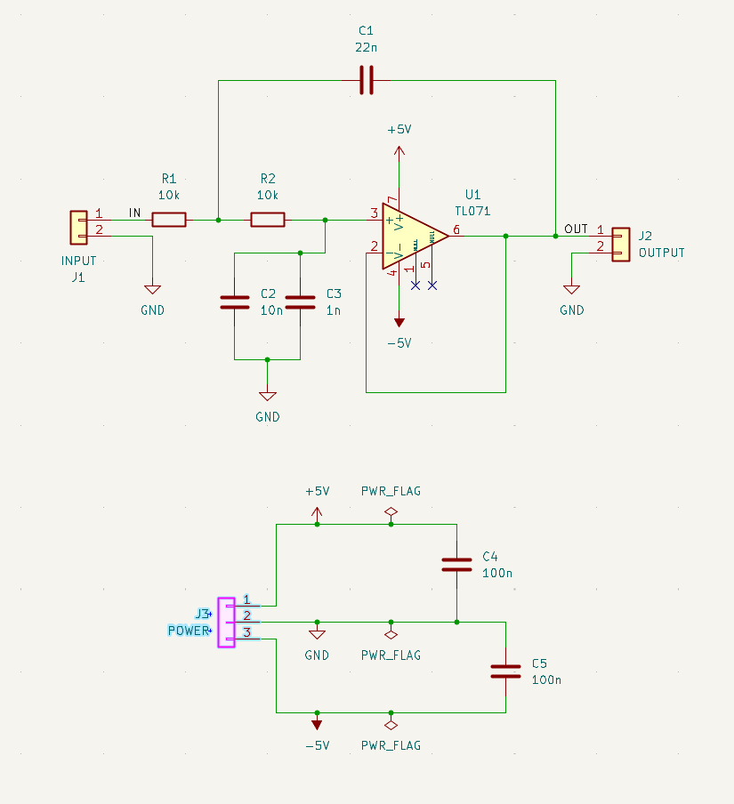
- The 11 nF capacitor. 11 nF isn't a value distributors stock. I split it into a 10 nF and a 1 nF in parallel, which adds up to exactly 11 nF and keeps the cutoff where the math says it should be.
- The voltage sources. V1, V2, and V3 became three pin headers: a signal input, a signal output, and a ±5 V power input for a bench supply.
- Decoupling. I added a 100 nF capacitor on each supply rail, placed as close to the op-amp's power pins as possible. Ideal op-amps don't need this; real ones do.
I also specified C0G/NP0 ceramics for the three filter capacitors so the cutoff frequency doesn't drift with temperature or voltage.
Schematic capture
I redrew the circuit in KiCad's schematic editor with the real parts, using power symbols for the supply rails and PWR_FLAGs so the checker knows where power enters the design. The filter section on top mirrors my LTspice schematic; the power section below is new.
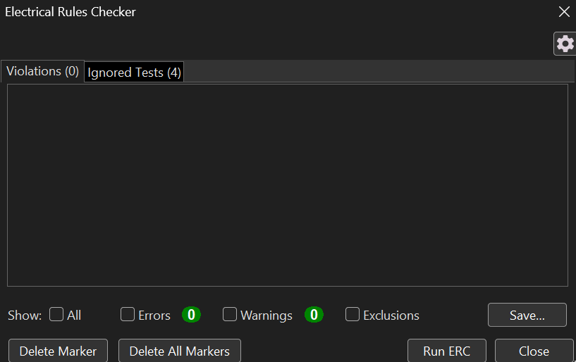
Before moving on, I ran the Electrical Rules Checker. It flags unconnected pins, missing power sources, and wires that look connected but aren't.
Assigning footprints
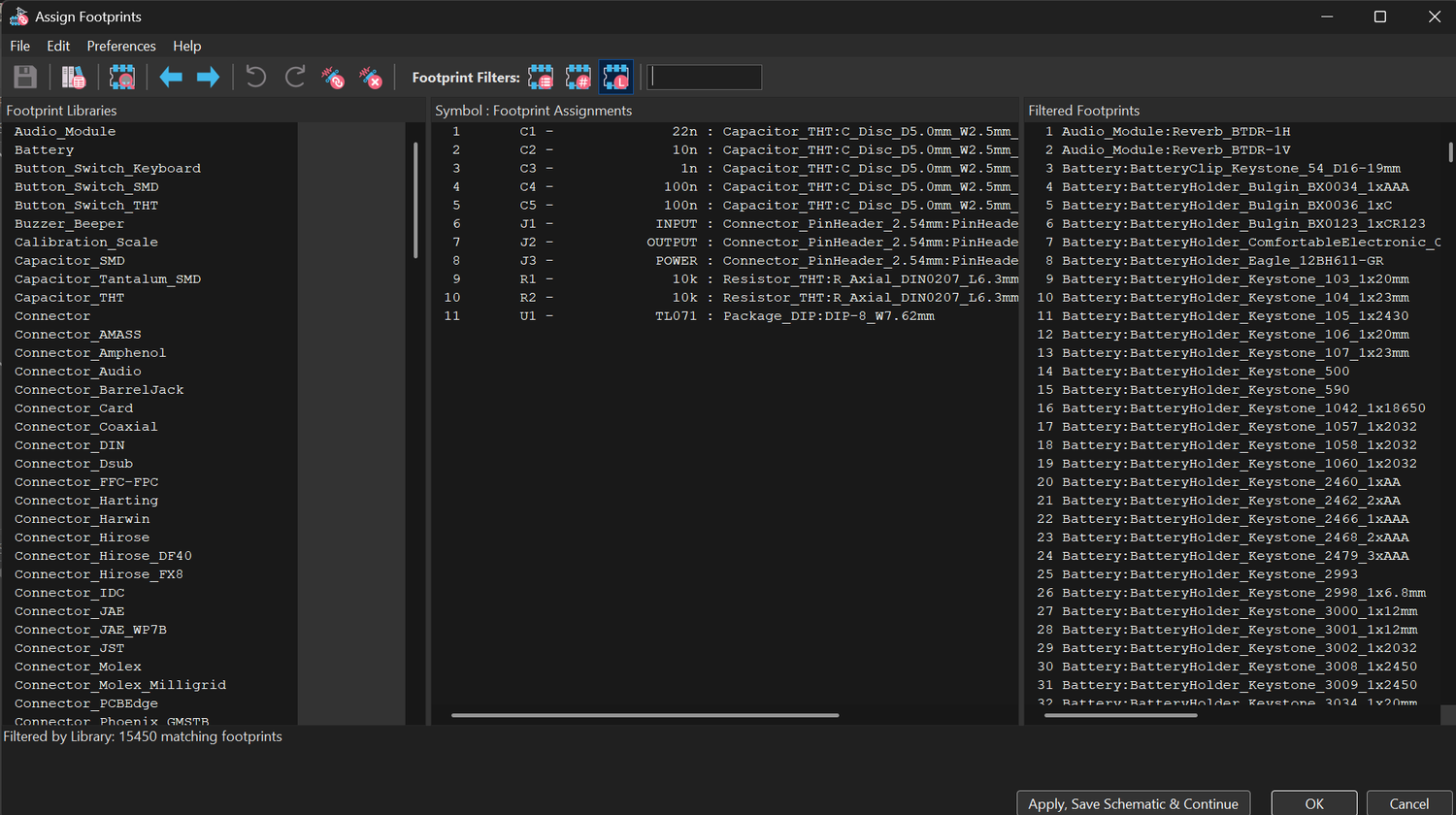
Each symbol has to be linked to the physical copper pattern it will be soldered to. I picked through-hole footprints for everything: axial resistors, 5 mm disc capacitors, a DIP-8 for the op-amp, and 2.54 mm pin headers for the connectors.
Placement
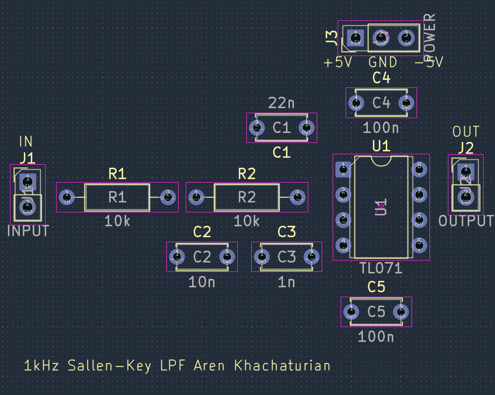
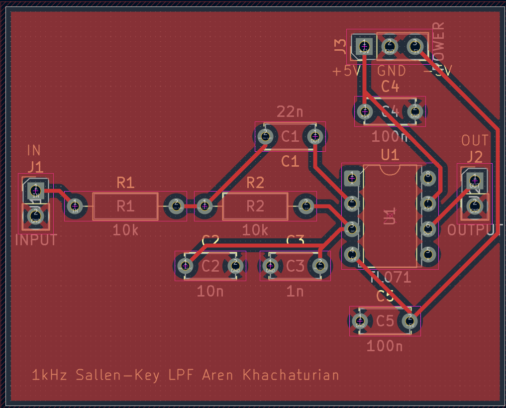
With the parts pulled into the PCB editor, I placed them so the signal flows left to right: input header, R1, R2, the op-amp, output header. C1 sits above the op-amp where its two connections are short, C2 and C3 sit right at the non-inverting input, and the two decoupling capacitors hug the supply pins. The thin white ratsnest lines show every connection that still needs a copper track.
Routing
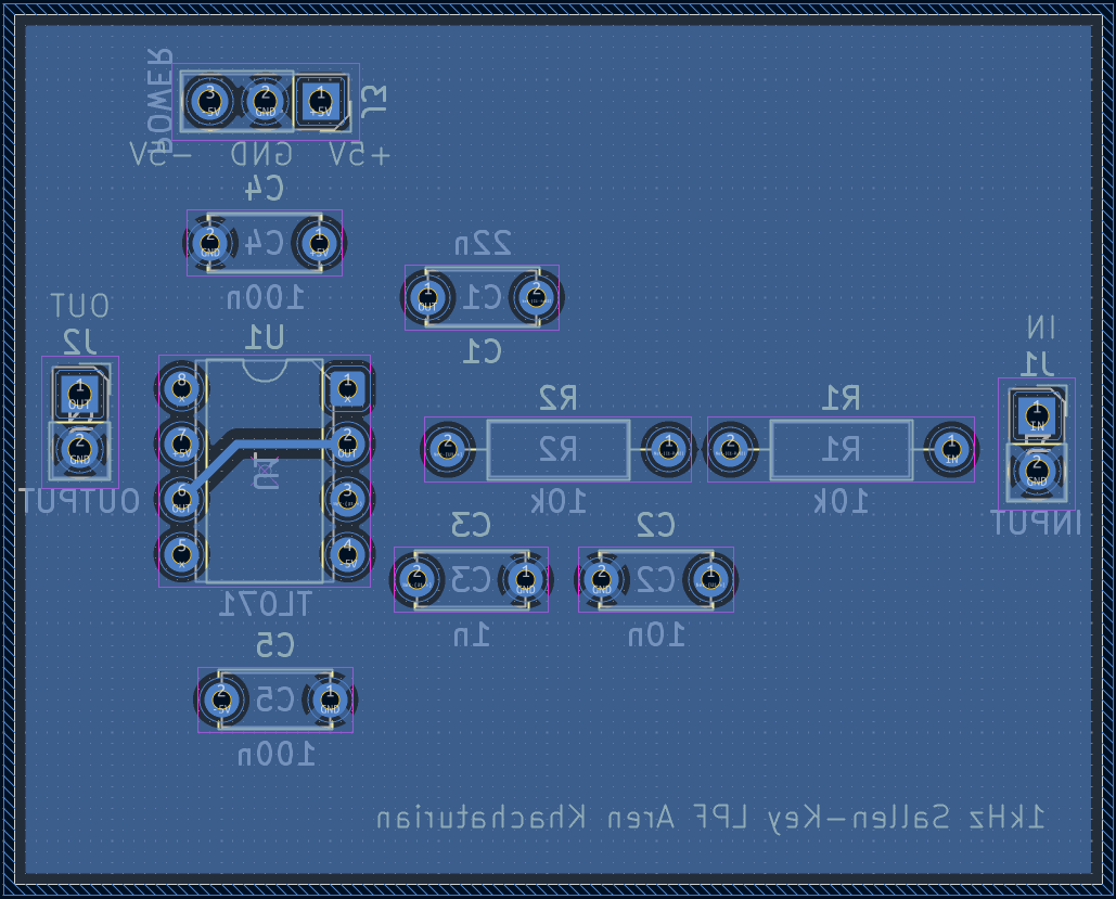
Almost every connection fit on the front copper layer. The one exception is the feedback link from the op-amp's inverting input (pin 2) to its output (pin 6), which has to cross under the chip. I routed that single trace on the back layer instead of forcing it around the outside of the package. Ground was left unrouted on purpose, because a copper pour handles it.
Ground planes
I filled both layers with a GND copper zone. Every ground pad connects to the pour through thermal-relief spokes rather than solid copper, so the pads can be hand-soldered without the plane pulling the heat away. Two planes tied together through the ground through-holes give the op-amp a quieter reference than a few thin ground tracks would.
Design rule check
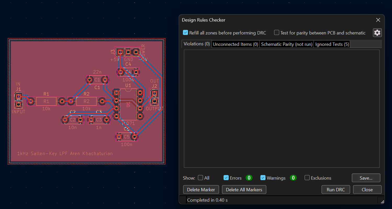
The Design Rules Checker compares the board against the fab's minimum clearances and confirms every net is complete. My first run turned up two problems, which is the point of running it: a ground pad near the board edge was only getting one thermal spoke because a −5 V trace was crowding it, and a 0.77 mm stub of track had been left dangling from an abandoned route. I moved the trace, removed the stub, refilled the zones, and re-ran the check.
Final DRC result: zero violations and zero unconnected items. Every net that exists in the schematic exists on the board.
Result
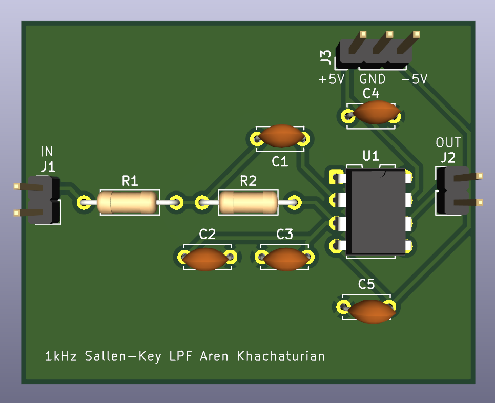
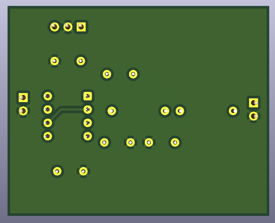
KiCad's 3D viewer renders the finished board with its parts, which is a fast way to catch a backwards connector or a mislabeled silkscreen before spending money on a fab run. I then generated the Gerber and drill files the manufacturer needs.
What I learned
- How to translate an idealized simulation into real, purchasable parts, and why decoupling capacitors matter on a physical board even when a simulator never asks for them.
- The full KiCad workflow from a blank project to fab files: schematic capture, ERC, footprint assignment, placement, routing, copper zones, DRC, and Gerber export.
- That placement is most of the work. Following the signal path and keeping decoupling tight made routing simple, with only one trace needing the back layer.
- Why ground pours use thermal reliefs, and how a copper zone can quietly fail to reach a pad when tracks crowd it.
- To treat DRC and ERC as part of the design, not a formality. Both caught real mistakes I would not have seen by looking at the board.
Next steps
This was a virtual project, so the board hasn't been ordered yet. The next step is to fabricate and assemble it, then measure the real cutoff with a function generator and oscilloscope and compare it against the 1,023 Hz from simulation. Component tolerances should put it within a few percent.